DATA SHEET
MJE13005
NPN SILICON
POWER TRANSISTOR
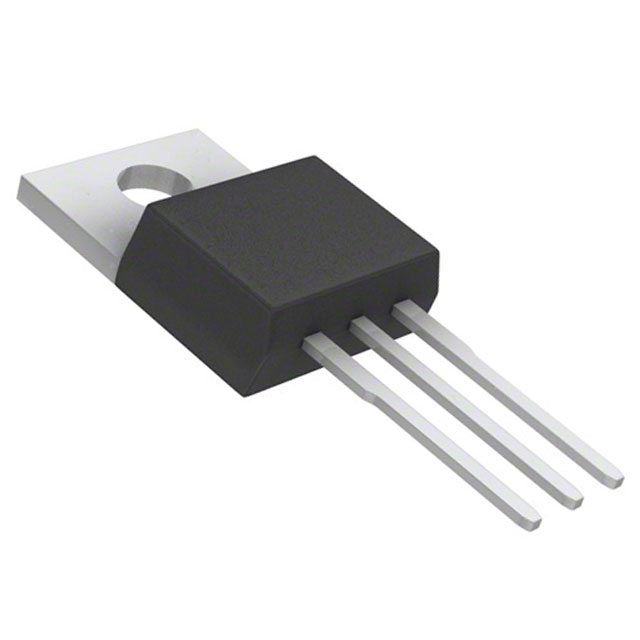
JEDEC TO-220 CASE
DESCRIPTION
The CENTRAL SEMICONDUCTOR MJE13005 is a Silicon NPN Power Transistor, designed for high speed power
switching applications.
MAXIMUM RATINGS (TC=25°C unless otherwise noted)
SYMBOL
Collector-Emitter Voltage
VCEO
Collector-Emitter Voltage
VCEV
Emitter-Base Voltage
VEBO
Collector Current
IC
Peak Collector Current
ICM
Base Current
IB
Peak Base Current
IBM
Emitter Current
IE
Peak Emitter Current
IEM
Power Dissipation (TA=25°C)
PD
Power Dissipation
PD
Operating and Storage
Junction Temperature
TJ,Tstg
Thermal Resistance
ΘJA
Thermal Resistance
ΘJC
UNITS
V
V
V
A
A
A
A
A
A
W
W
400
700
9.0
4.0
8.0
2.0
4.0
6.0
12
2.0
75
-65 to +150
°C
62.5
°C/W
1.67
°C/W
ELECTRICAL CHARACTERISTICS (TC=25°C unless otherwise noted)
SYMBOL
TEST CONDITIONS
ICEV
ICEV
IEBO
BVCEO
VCE(SAT)
VCE(SAT)
VCE(SAT)
VBE(SAT)
VBE(SAT)
hFE
hFE
VCE=700V, VBE(OFF)=1.5V
VCE=700V, VBE(OFF)=1.5V, TC=100°C
VEB=9.0V
IC=10mA
IC=1.0A, IB=0.2A
IC=2.0A, IB=0.5A
IC=4.0A, IB=1.0A
IC=1.0A, IB=0.2A
IC=2.0A, IB=0.5A
VCE=5.0V, IC=1.0A
VCE=5.0V, IC=2.0A
MIN
MAX
UNITS
1.0
5.0
1.0
mA
mA
mA
V
V
V
V
V
V
400
10
8.0
0.5
0.6
1.0
1.2
1.6
60
40
(Continued)
R1
�MJE13005
NPN POWER TRANSISTOR
ELECTRICAL CHARACTERISTICS (CONTINUED)
TEST CONDITIONS
SYMBOL
MIN
fT
Cob
VCE=10V, IC=500mA, f=1.0MHz
VCB=10V, IE=0, f=100kHz
td
Resistive Load
VCC=125V, IC=2.0A, IB1= IB2=0.4A
TYP
4.0
tsv
tc
UNITS
MHz
pF
130
0.1
µs
0.7
4.0
0.9
µs
µs
µs
Inductive Load
IC=2.0A, Vclamp=300V, IB1=0.4A,
4.0
µs
VBE(off)=5.0V, TC=100°C
0.9
µs
tp=25µs, Duty Cycle ≤ 1.0%
tr
ts
tf
MAX
tfi
0.16
µs
TO-220 PACKAGE - MECHANICAL OUTLINE
A
DIMENSIONS
INCHES
MILLIMETERS
SYMBOL MIN
MAX
MIN
MAX
A
0.170 0.190
4.31
4.82
B
0.045 0.055
1.15
1.39
C
0.013 0.026
0.33
0.65
D
0.083 0.107
2.10
2.72
E
0.394 0.417 10.01 10.60
F (DIA)
0.140 0.157
3.55
4.00
G
0.100 0.118
2.54
3.00
H
0.230 0.270
5.85
6.85
I
0.560 0.625 14.23 15.87
J
0.250
6.35
K
0.025 0.038
0.64
0.96
L
0.500 0.579 12.70 14.70
M
0.090 0.110
2.29
2.79
TO-220 (REV: R2)
E
F
B
G
H
I
1 2 3
J
C
D
L
K
Lead Code:
M
R2
1) Base
2) Collector
3) Emitter
Tab is Common to Pin 2
�OUTSTANDING SUPPORT AND SUPERIOR SERVICES
PRODUCT SUPPORT
Central’s operations team provides the highest level of support to insure product is delivered on-time.
• Supply management (Customer portals)
• Custom bar coding for shipments
• Inventory bonding
• Custom product packing
• Consolidated shipping options
DESIGNER SUPPORT/SERVICES
Central’s applications engineering team is ready to discuss your design challenges. Just ask.
• Free quick ship samples (2nd day air)
• Special wafer diffusions
• Online technical data and parametric search
• PbSn plating options
• SPICE models
• Package details
• Custom electrical curves
• Application notes
• Environmental regulation compliance
• Application and design sample kits
• Customer specific screening
• Custom product and package development
• Up-screening capabilities
REQUESTING PRODUCT PLATING
1. If requesting Tin/Lead plated devices, add the suffix “ TIN/LEAD” to the part number when
ordering (example: 2N2222A TIN/LEAD).
2. If requesting Lead (Pb) Free plated devices, add the suffix “ PBFREE” to the part number
when ordering (example: 2N2222A PBFREE).
CONTACT US
Corporate Headquarters & Customer Support Team
Central Semiconductor Corp.
145 Adams Avenue
Hauppauge, NY 11788 USA
Main Tel: (631) 435-1110
Main Fax: (631) 435-1824
Support Team Fax: (631) 435-3388
www.centralsemi.com
Worldwide Field Representatives:
www.centralsemi.com/wwreps
Worldwide Distributors:
www.centralsemi.com/wwdistributors
For the latest version of Central Semiconductor’s LIMITATIONS AND DAMAGES DISCLAIMER,
which is part of Central’s Standard Terms and Conditions of sale, visit: www.centralsemi.com/terms
w w w. c e n t r a l s e m i . c o m
(001)
�
很抱歉,暂时无法提供与“MJE13005 PBFREE”相匹配的价格&库存,您可以联系我们找货
免费人工找货